Microsoft Infrastructure - AI & CPU Custom Silicon Maia 100, Athena, Cobalt 100
Length: • 10 mins
Annotated by Umer
Microsoft is currently conducting the largest infrastructure buildout that humanity has ever seen. While that may seem like hyperbole, look at the annual spend of mega projects such as nationwide rail networks, dams, or even space programs such as the Apollo moon landings, and they all pale in comparison to the >$50 billion annual spend on datacenters Microsoft has penned in for 2024 and beyond. This infrastructure buildout is aimed squarely at accelerating the path to AGI and bringing the intelligence of generative AI to every facet of life from productivity applications to leisure.
While the majority of the AI infrastructure is going to based on Nvidia’s GPUs in the medium term, there is significant effort to diversify to both other silicon vendors and internally developed silicon. We detailed Microsoft’s ambitious plans with AMD MI300 in January and more recently the MI300X order volumes for next year. Outside of accelerators there are also significant requirements for 800G PAM4 optics, coherent optics, cabling, cooling, CPUs, storage, DRAM, and various other server components.
Today we want to dive into Microsoft’s internal silicon efforts. There are 2 major silicon announcements for today’s Azure Ignite event, the Cobalt 100 CPUs and the Maia 100 AI accelerators (also known as Athena or M100). Microsoft’s systems level approach is very notable, and so we will also go into rack level design for Maia 100, networking (Azure Boost & Hollow Core Fiber) and security. We will dive into Maia 100 volumes, competitiveness with AMD MI300X, Nvidia H100/H200/B100, Google’s TPUv5, Amazon’s Trainium/Inferentia2, and Microsoft’s long-term plans with AI silicon including the next generation chip. We will also share what we hear about GPT-3.5 and GPT-4 model performance for Maia 100.
It should be noted that while Microsoft is currently behind on deploying custom silicon in their datacenters relative to Google and Amazon, they have a long history of silicon projects. For example, did you know that Microsoft developed their own custom CPU called E2 with a custom instruction set that utilized EDGE (Explicit Data Graph Execution). They even ported Windows specifically for this ISA! Microsoft has historically worked with AMD on semi-custom gaming console chips, but they are also now extending partnerships to custom Arm based Windows PC chips. Microsoft has also internally developed multiple generations of root of trusts that are found on every single server they install in their datacenters.
Microsoft Project Catapult for a long time which targets search, AI, and networking. Initially Project Catapult was based entirely on standard FPGAs, but Microsoft eventually engaged with Intel for a custom FPGAs. The purpose of this FPGA was primarily for Bing, but it had to be scrapped due to Intel’s execution issues. Bing still relies heavily on FPGAs, in contrast to Google search which is primarily accelerated by TPUs.
As part of the announcements today, Microsoft is also announcing the Azure Boost network adaptor, which is a 200G DPU based on an external FPGA and an internally designed ASIC. This product offloads many hypervisor, host, network, and storage related tasks, but for some reason Azure instances with Azure boost still have to give up host CPU cores for infrastructure related tasks. This differs from Amazon’s Nitro which frees up all host CPU cores for VMs.
Azure Cobalt 100 CPU
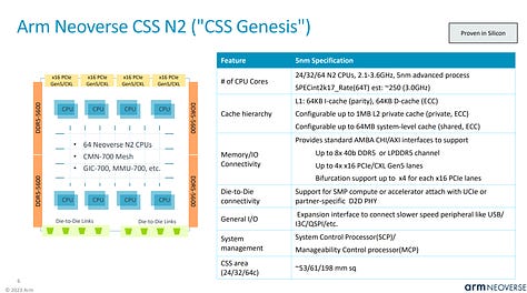
The Azure Cobalt 100 CPU is Microsoft’s 2nd Arm based CPU that they have deployed in their cloud. It is already being used for internal Microsoft products such as Azure SQL servers and Microsoft Teams. The first Arm based CPU Microsoft deployed was a Neoverse N1 based CPU purchased from Ampere Computing. The Cobalt 100 CPU evolves from that and brings 128 Neoverse N2 cores on Armv9 and 12 channels of DDR5. Neoverse N2 brings 40% higher performance versus Neoverse N1.
Cobalt 100 is primarily based on Arm’s Neoverse Genesis CSS (Compute Subsystem) Platform. This offering by Arm diverges from their classic business model of only licensing IP and makes it significantly faster, easier, and lower cost to develop a good Arm based CPU.
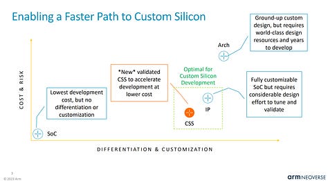

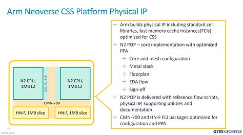
Arm provides verified and laid out blobs that have many aspects of the design process completed for vendors. We detailed this new business model more here.
In the case of Cobalt 100, Microsoft is taking 2 Genesis compute subsystems and tying them together into 1 CPU.
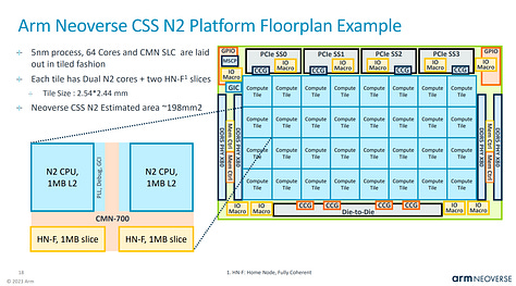
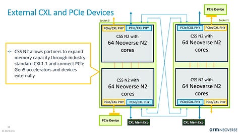
This is similar to Alibaba’s Yitan 710 CPU, which is also based on Neoverse N2. Chips and Cheese profiled that here.
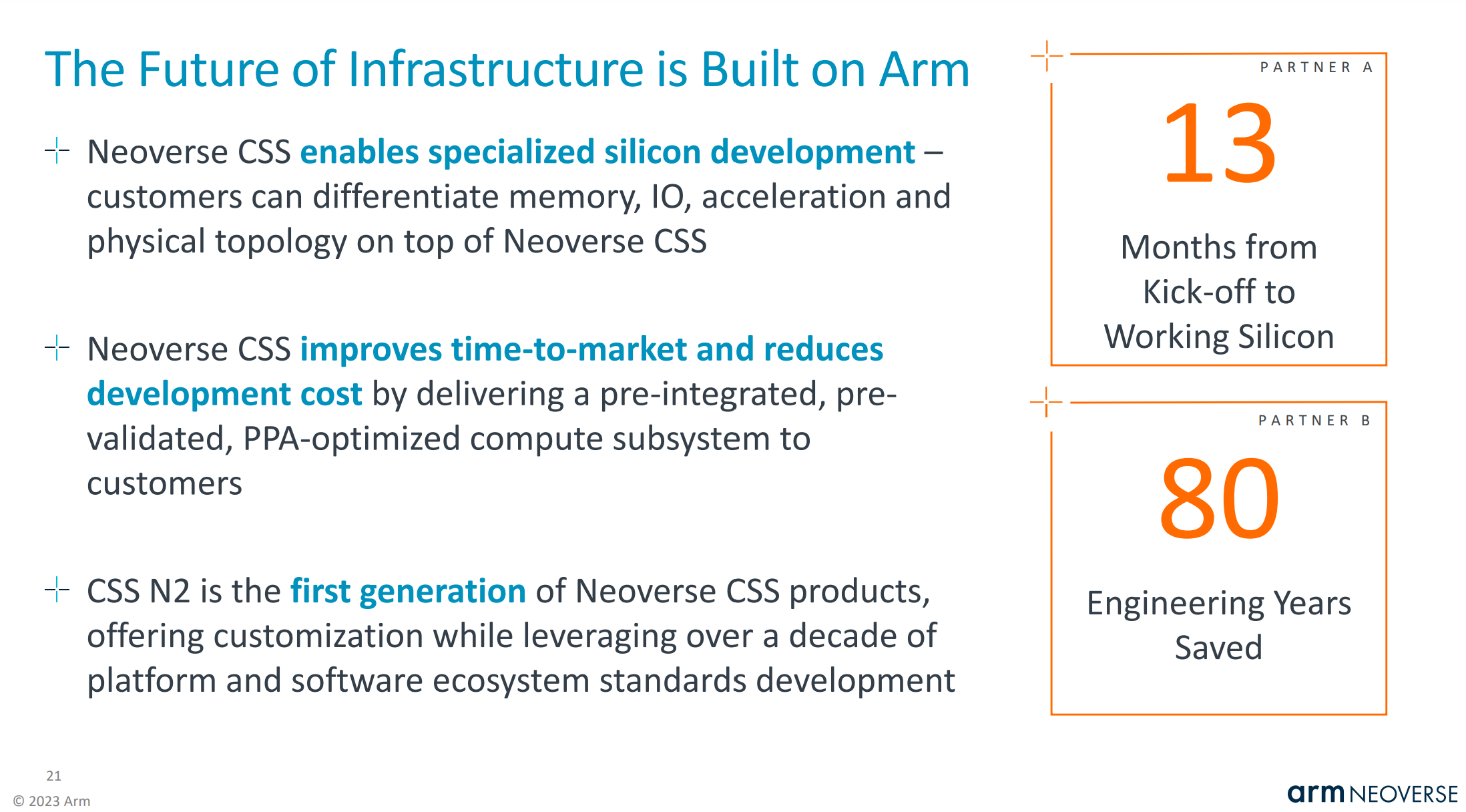
Arm has previously bragged that it only took 13 months from the kick-off of a project to having working silicon for a hyperscaler. Given Alibaba and Microsoft are the only customers for Genesis CSS that we know of, and Alibaba was the first to market, it is likely that Arm is talking about Microsoft on the slide below. There is also a possibility that Google’s Arm based CPU is using Genesis CSS as well.
Azure Maia 100 (Athena)
Microsoft’s long awaited AI accelerator is finally here. They are the last of the big 4 US hyperscalers (Amazon, Google, Meta, Microsoft) to unveil their product. With that said, Maia 100 isn’t a slouch. We will compare its performance / TCO versus AMD MI300X, Nvidia H100/H200/B100, Google’s TPUv5, Amazon’s Trainium/Inferentia2.
The bulk of this piece is below. It will include the full specifications, network setup and topology, rack design, volume ramp, performance, power consumption, design partners, and more. There are some very unique aspects of this chip that we think ML researchers, infrastructure folks, silicon design teams, and investors should be made aware of.
Let’s start off with the raw specs of the chip. It is made on TSMC’s 5nm node and is a monolithic die with 105 billion transistors. This is the highest transistor count monolithic die that has every been disclosed publicly.
Starting off with FLOPS, Maia comes with 1600 TFLOPS of MXInt8 and 3200 TFLOPS of MXFP4. Note while the number formats being used here are unique, the hope is that MXInt8 is a drop in for FP16/BF16 and MXFP4 is a drop in for FP8, at least for inference. This is extremely handwavy, but an okay heuristic for now given no one has actually trained massive models with these number formats. We are currently doing a deep dive on numeric formats given the advent of the new OCP standard and adoption of it in the future, so stay tuned for that. Frankly, waffling about the disadvantages and advantages of number formats here would take way too long and is beyond scope.
The FLOPS of this chip outright crush Google’s TPUv5 (Viperfish) as well as Amazon’s Trainium/Inferentia2 chips. Surprisingly it’s not even that far off from Nvidia’s H100 and AMD’s MI300X in that department.
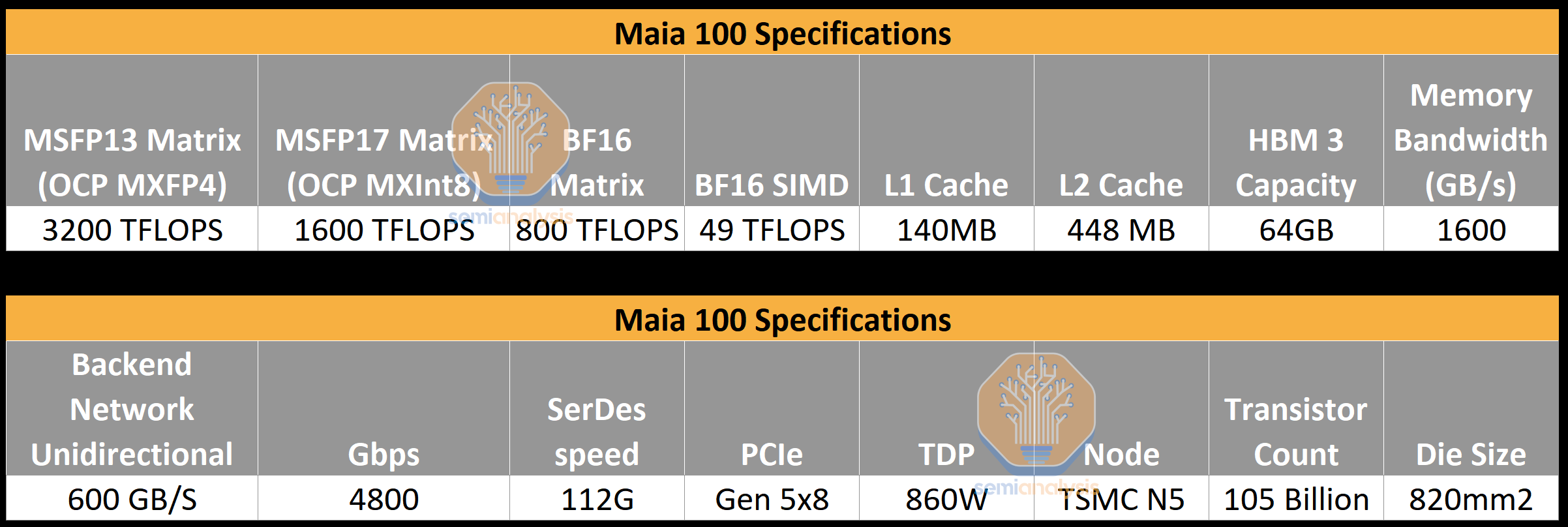
The more relevant spec here is the memory bandwidth at 1.6TB/s. This still crushes Trainium/Inferentia2, but it is less memory bandwidth than even the TPUv5, let alone the H100 and MI300X. Microsoft unfortunately underspecced Maia 100 in memory bandwidth.
This is because the chip was designed before the LLM craze happened. As such Maia is a bit unbalanced in terms of on die memory vs off die memory. Microsoft put a load of SRAM on the chip, because large amounts of SRAM make sense for some model architectures. Large caches generally help reduce the memory bandwidth that is required, but that doesn’t apply to large language models.
Microsoft is effectively spending expensive die area on something that doesn’t help in its primary workload. Note AMD did the same with MI300 as we discussed here, although they did that primarily for the HPC market. AMD still went to the max with memory bandwidth, which blunts the harm, and really only increases their manufacturing cost. Microsoft made the tradeoff of going with 4 stacks of HBM instead of 6 like Nvidia and 8 like AMD.
The other really interesting aspect of this design is what Microsoft did with networking. In the case of AMD and Nvidia, they have their Infinity Fabric and NVLink for high speed connectivity to a small number of nearby chips, generally 8 although Nvidia has some deployments that go up to 256 currently. To connect tens of thousands of GPUs together, Nvidia and AMD require going out PCIe to network add in cards for Ethernet/InfiniBand.
Microsoft took a different path entirely, more similar to what Intel is doing with their Gaudi line of accelerators. Each chip has its own built in RDMA Ethernet IO. This sums up for a total of 4.8Tbps per chip IO, which beats both Nvidia and AMD. This is similar to what Google has done with their TPUv5 and their proprietary ICI network.
Note that this 4.8T is unidirectional, which is the standard for measuring networking speeds. When you play with Nvidia math on their NVLink, that’s actually 9.6T vs the H100/H200’s 7.2T. Microsoft’s Maia 100 actually has more scale up bandwidth than Nvidia which is very impressive. Note that the Maia 100 cut PCIe lanes down to 8 in order to maximize the beachfront area for 112G SerDes. Nvidia has 16 lanes because they need those to connect to Ethernet/InfiniBand. Nvidia also spends beachfront area on their C2C which is used to connect Grace CPUs to Hopper GPUs at high bandwidth. If we include that short reach point to point interconnect, then Nvidia is still ahead.
For those keeping track, Maia 100 is within spitting distance in FLOPS, leading the pack in network IO, and behind Nvidia and AMD in memory bandwidth. Compared to Amazon, who is currently on their 2nd generation chip, Microsoft on paper crushes them on every metric. Amazon will be coming with their third generation AI chips, Trainium 2 and Inferentia 3 next year, but the noteworthy item is that Microsoft’s silicon team is already competitive with Amazon’s right out the gate. Undoubtedly, Microsoft silicon teams are also getting more feedback from OpenAI than Anthropic is giving Amazon, so all of this bodes well for the future and continues to lend more credence the Amazon Cloud Crisis thesis.
Of course, paper specs are nice, but what matters is actually deployed.
Ares Rack and Cluster Architecture
Microsoft’s rack and cluster design for Maia (Athena) is called Ares. These racks are highly customized to Maia and are not standard 19” or OCP racks as they are much wider. There are 4 Maia accelerators per server. There are 32 Maia chips across 8 servers in a rack.
Maia is only deployed in watercooled configurations. In datacenters that support watercooling, this is straight forward, and facilities water can hook into a water to water exchanger. In datacenters that do not support watercooling, Microsoft has to deploy water to air CDUs. The Maia racks seem to require ~40KW, which is more than most legacy datacenters which still only support ~12KW racks.
Alongside the 8 Maia servers also sits network switches. Arista and Cisco seem to be dual sourced for these top of rack switches. There are a total of 3 different switches in the rack. Microsoft is utilizing the dual ToR design that we discussed here. This includes utilizing Y cables that used to be primarily sourced from Credo, but others have already been qualified and put into production as well.

Each Maia server has 12 400G Ports that go to the backend network. There are also 2 100G ports that go to the frontend network.
The largest individual deployment for the backend network for Maia is 2,048, but there is nothing preventing them from scaling this up further. Note it will be deployed in multiple datacenters, and some datacenters will have multiple. With that said, volumes for this chip are quite low relative to Microsoft’s orders of AMD and Nvidia chips. For specific volumes, contact us for our accelerator model which flows through HBM and CoWoS production, packages per wafer, yields, volumes by chip type, and revenue for fabless design companies/backend design partners.
It should be noted that Amazon is buying and deploying far more of their Trainium and Inferentia2 chips despite them being inferior to Microsoft’s Maia. This is because Amazon has relatively lower allocations of Nvidia GPUs and also because Amazon believes in subsidizing their own parts to get the external ecosystem going. Contrast this with Microsoft whose AI accelerators are primarily for internal workloads, because they actually have a strong AI services and API business. This means Microsoft will pick the best TCO chip rather than subsidize a loss leader like Amazon.
Something noteworthy is that Microsoft is not using any backend design partner for these chips. They are licensing the SerDes themselves from a 3rd party rather than relying on a backend partner like Broadcom or Marvell. They are submitting the design directly to TSMC. They are designing the package. This is an all Microsoft design. Microsoft is leveraging GUC for supply chain management, but GUC is not involved in the design at any point. For those bidding up GUC’s Taiwan stock due to their collaboration with Microsoft, simmer down, the margins will be extremely low because GUC is effectively just a balance sheet.
GPT-3.5 and 4 Performance/TCO
The important thing to watch is performance. Microsoft is still working on the software stack of course, which we discussed in detail here back in January.
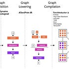
It is still maturing, but the area they are directing their attention is LLM inference. This also applies for the AMD MI300X. Training is simply much more complicated on the software front.
On the inference side, note that the memory tradeoffs that Microsoft made are hugely penalizing. This makes it very difficult for Microsoft to compete. H100 has a bit more than 2x the memory bandwidth, H200 has 3x the memory bandwidth, and MI300X even more. Hence for LLM inference, Maia 100 is in a tough position for performance. The performance in GPT-4 inference is roughly 1/3 that of the H100 in terms of high batch size tokens per second.
Note this isn’t a huge issue alone because the manufacturing costs vs Nvidia’s huge margins make up for most of this gap. The problem is that power and cooling are still relevant costs, and the token to token latency is worse. In latency sensitive applications such as chatbot and many co-pilot tools, there is no way for Maia to compete with Nvidia and AMD GPUs. Both those GPUs can turn to using larger batch sizes, while still having acceptable latency, so their utilization will be higher and the performance TCO is much better vs Maia.
In smaller models like GPT 3.5 turbo, the story is a bit better, but Microsoft can’t deploy hardware that is clearly sub-optimal for large models because small models like 3.5 turbo will be phased out over time.
Next Generation Maia
As far as the next generation goes, Athena is replaced by Braga. This chip will move to have the correct ratios of on die cache vs HBM. Unfortunately for Microsoft, that is more of a late 2025 or 2026 product, which means its not competing with H100, or H200, or B100, but rather Nvidia’s X/R100. We have hope for Microsoft’s internal AI silicon going forward, because the first attempt was quite strong, but this treadmill / rat race is not easy.
Hollow Core Fiber
Microsoft is also claiming to be deploying hollow core fibers. We aren’t sure how impressive this is, but it is interesting. Hollow core is when the central core of a fiber is engineered with a lattice of air holes rather than a solid dielectric material typically found in standard optical fibers. Theoretically, light traveling through air experiences less latency compared to glass. Reducing intra-datacenter latency is a must for multi-datacenter training.