Through the Ages: Apple CPU Architecture
Length: • 24 mins
Annotated by howie.serious
howie.serious: 一句话总结: 本文详细讲述了苹果CPU架构的四个时期,包括其背后的基本CPU概念。 🖥️ **关键词1:苹果CPU架构** :本文通过讲述苹果CPU架构的四个时期,展示了苹果如何通过不断创新和优化硬件,使其产品保持竞争力。 📈 **关键词2:基本CPU概念** :文章中详细解释了一些基本的CPU概念,如寄存器,算术逻辑单元,8位与16位,CISC与RISC,流水线,汇编语言,仿真,CPU缓存,分支预测,超标量架构,超线程,异构计算等。 🍎 **关键词3:苹果的创新** :苹果凭借其对硬件的极致追求和创新,成功地从Mac的发布开始,三次完成了其CPU架构的迁移。 1. 苹果如何通过创新和优化础硬件来保持其产品的竞争力? 2. 什么是基本的CPU概念,它们是如何影响计算机性能的? 3. 苹果是如何在历史上完成其CPU架构的迁移的?
Learn how CPUs work, and discover Apple’s underrated competitive advantage.
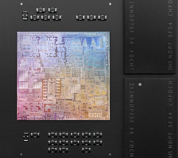
Timeline & Key Concepts
This is the tale of the 4 Ages of Apple CPU Architecture. Each chapter, however, also serves as a framing device for fundamental CPU concepts.
If Android is more your thing, you are free to jump between sections at will like an overclocked instruction pointer.
1984 — Motorola 68k
1994 — PowerPC
2006 — Intel x86
2020 — Apple Silicon
- Heterogeneous Computing
- Unified Memory Architecture
- Out-of-order Execution
- Physics: The Ultimate Constraint
The King of CPU Architecture Migrations
I’m no evangelist, but it doesn’t take a fanboy to acknowledge that Apple is an impressive company.
They invented the most successful product in the history of capitalism, and subsequently became the first business to hit a $1T market cap. Through hit products like the iPod, unparalleled branding, and the reality distortion field of Steve Jobs, they even managed to make tech cool.
Behind this impressive execution is a borderline-obsessive hardware optimisation: Since the Mac was released in 1984, Apple has migrated its CPU architecture three times.
This is no easy feat.
Every time a computer company announces a CPU architecture migration, there is widespread skepticism about whether the business can survive its entire software ecosystem being deprecated at once.
In the days when software still came in cardboard boxes, this skepticism bordered on incredulity. John Dvorak, prominent tech columnist, suggested the 2005 move to Intel x86 was a precursor to bringing Apple onto Windows.
Apple is the undisputed king of CPU architecture migrations.
Apple’s tolerance for pain in the short term has allowed them to master the processor game. Each new CPU architecture allowed Apple to stay competitive against existential threats; or to place themselves head-and-shoulders above the competition.
Today, we’re going on an odyssey through the 4 eras of Apple CPU architectures. I’ll colour in the business context — why each migration was necessary — and will show you how Apple survived each transition to end up even stronger than before.
Along the way, we’ll learn some critical CPU concepts as we go. Chip technology becomes more and more advanced as time marches on, offering us a convenient learning curve as we travel Through The Ages.
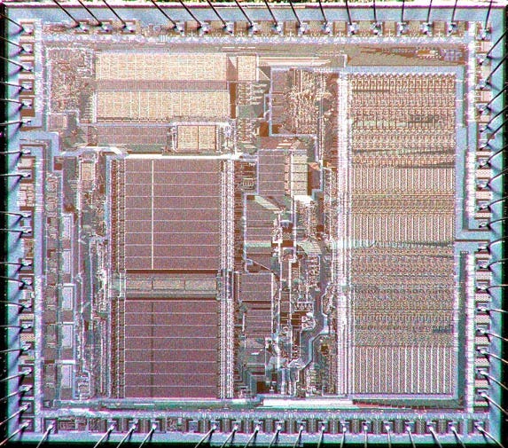
1984 — Motorola 68k
1981.
Reagan. MTV. Indiana Jones.
Apple is stumbling.
Its early breakout success and cash cow, the Wozniak wizardry of the 1977 Apple II, was creaking under its age.
The IBM PC has just hit the mass market, precipitating an unprecedented influx of purchase orders for PCs. 24-year-old whizkid Bill Gates was asked to supply IBM’s operating system.
In 10 years, let’s check in on our friends at IBM to see how this move went.
Apple’s LISA is shaping up to be their flagship product. After being a huge jerk to everybody for 5 years, Steve Jobs has been relegated by the board to run the low-end Macintosh project.
Choosing a CPU
Initially a cheaper mass-market consumer product, the Macintosh under Jobs pivoted to focus on one thing: upstaging the LISA team. Steve introduced a cutting-edge totally-not-stolen graphical user interface to the Macintosh and demanded his team find the most advanced hardware available at the time.
If you want to make a dent in the personal computer universe, your choice of CPU is critical. This is the hardware in which your OS lives and the platform upon which you nurture your software ecosystem.
Very early PCs — the sort that hobbyists like Wozniak assembled in their garages — used 8-bit CPUs. But if you’re designing a powerful mass-market computer in the early 1980s, you’re going to want to use modern 16-bit processor architecture. There are really three major choices available: The Intel 8088, the Zilog Z8000, or the Motorola 68k.
Here, 8-bit and 16-bit refers to the size, or “width” in bits, of the registers and data bus with which the CPU works.
The CPU and Registers
Let’s get on the same page: a CPU is a device that moves data from computer memory (RAM) into fast temporary memory (registers), runs operations on this data, then moves the output back into memory.
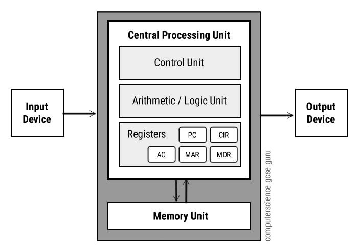
A register is the tiniest unit of electronic memory — they each hold just a few bits in the heart of the CPU. The CPU follows instructions (a computer program) to perform operations on this data — manipulating the bits (1s and 0s).
The ALU
These operations are performed by the Arithmetic-Logic Unit (ALU). This is basically a collection of circuits that perform simple, specialised jobs, such as:
- Adding up binary numbers, e.g.
0010+0101=0111 - Perform logical operations, e.g.
NOT0000=1111 - Shift bits around, e.g. left-shifting
0011by 1 place becomes0110
The CPU’s control unit decodes instructions one at a time to decide what data should move to which register, and which register’s data should go through which ALU circuitry.
Perform these operations lots of times, very quickly, and it adds up to outputs such as matrix multiplication, collision physics in a video game, or rasterising image data into on-screen pixels.
8-bit and 16-bit
So why does bit width matter?
An 8-bit CPU can run a NOT operation on 0010110 in one clock cycle, inverting its bits into 1101001. A 16-bit CPU leaves this in the dust, converting a hefty 10100100010110 into 01011001101001 in the same amount of time.
Moreover, a single 8-bit register can point at 28 different byte ‘addresses’ in RAM — a meagre 256 locations in which we can look for data. Due to this limitation, most 8-bit computers needed two registers to store memory addresses. 16-bit registers, or two 8-bit registers stacked against each other, can point to 216 memory addresses, meaning access to 64kB of memory.
Endian-ness becomes a major compatibility consideration when upgrading from 8-bit (1 byte) to 16-bit CPUs (2 bytes). Systems are either big-endian or little-endian, which defines the order in which they store bytes — for example, the number 41,394, in hexadecimal fashion, would be stored on registers as A1 B2 in big-endian systems and B2 A1 in little-endian systems.
Lastly, the “data bus” refers to the circuity that connects the CPU to main memory; so a 16-bit bus is essentially twice as fast as an 8-bit bus at reading and writing data to and from memory.
Are we all on the same page? Let’s get back to Apple.
Intel vs Zilog vs Motorola
Let’s imagine you’re Apple’s VP of Hardware presenting to Jobs.
Which chip architecture do you think you’d choose?
Intel 8088
- 8/16-bit microprocessor — 8-bit registers with a 16-bit data bus.
- 20-bit memory addressing range — supports 640kB of RAM.
- The IBM PC uses this chip architecture, so it has a strong existing software ecosystem.
- Low-end price point of ~$35 (in 1983 dollars) thanks to Intel’s massive economies of scale.
- Little-endian.
Zilog Z8000
- Pure 16-bit microprocessor — 16-bit registers and 16-bit data bus.
- 23-bit memory addressing rage — supports 8MB of RAM
- Few large competitors use this architecture, minimal software ecosystem.
- Mid-range price point of ~ $55 in 1983 dollars while looking to build market share.
- (Mostly) big-endian.
Motorola 68k
- 16/32-bit microprocessor — 32-bit registers with a 16-bit data bus.
- 24-bit memory addressing range —supports 16MB of RAM.
- Atari and Commodore use this chip architecture, some existing dev ecosystem.
- Prior supplier relationship with Motorola through the Apple I, Apple II, and LISA.
- Mid-to-high-end price point of ~$70 in 1983 dollars.
- Big-endian.
Overall, the Motorola 68k appeared to be the forward-thinking choice to show why 1984 won’t be like 1984. The weaker dev ecosystem and compatibility was a necessary sacrifice to provide brand differentiation against the dominant IBM PC.
What’s more, the 68k had a (mostly) orthogonal instruction set — this meant that (almost) every CPU operation could be performed on (almost) every register, whereas many competing CPUs had instructions restricted to specific registers. Orthogonality makes a CPU much easier to program, which is ideal when nurturing a nascent software ecosystem.
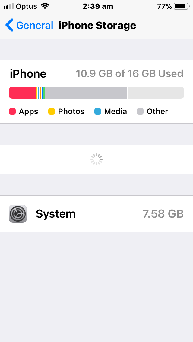
The 16MB addressing range ended up becoming critical: the Macintosh reserved the top 12MB of RAM for the OS, leaving a pithy 4MB of computer memory shared between software applications.
If you ever looked, dismayed, at the storage space available in your 16GB iPod Touch in 2012, you’ll know that nothing changes.
1994 — PowerPC
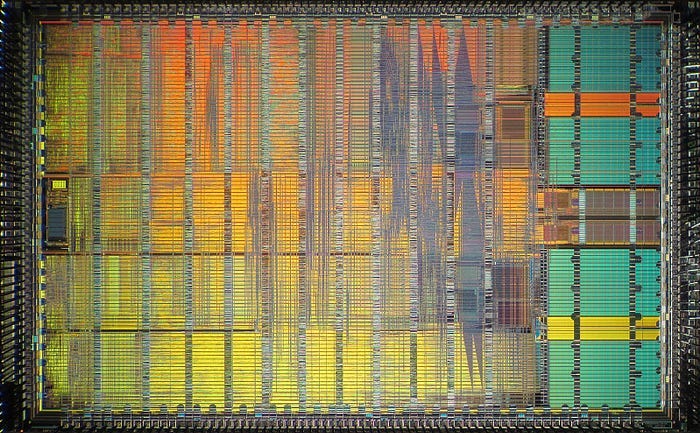
The year is 1994.
Steve Jobs was ousted by Apple 8 years ago, and is busy inventing Pixar and NeXT.
Apple is losing relevance.
Their former bitter PC rival, IBM, was in the long, painful process of having their lunch eaten by Microsoft.

Intel and Bill Gates, who was more commonly known as “the devil” in the 1990s, had entered an unholy marriage referred to as Wintelthat was carving out near-monopolies for both businesses.
Beyond consistent improvement to their powerful x86 chip architecture, Intel had just produced the greatest innovation since the transistor: giving their chip a cool name. The Pentium processor powered the Microsoft market-share munching machine.
That’s not to downplay the power of x86 chip architecture: Intel was earning its dominance with a 100MHz clock speeds and unparalleled power efficiency. The Motorola 68,000 chip family that carried the Macintosh into the 90’s was failing to keep up.
With the computer world under threat from monopoly, Apple joined up with its longtime partner, Motorola, and an unlikely ally, IBM. The plan: use the power of friendship to fight the forces of capitalism.
The AIM (Apple, IBM, Motorola) alliance was born. They realised that the x86 architecture had a key weakness: it utilised CISC architecture.
In response, AIM deployed a RISCy tactic: PowerPC.
CISC vs. RISC
There are two opposing chip design philosophies:
- CISC (Complex Instruction Set Computer)
- RISC (Reduced Instruction Set Computer)
To understand this, we need to get a handle on what is meant by Instruction Sets. In the previous section, I mentioned the CPU is running operations every clock cycle. These operations include things like moving data between registers, arithmetic, and logic operations.
Each CPU, constrained by the actual physical layout of its circuitry, can perform a limited number of different operations. These individual operations are represented by Assembly Language, also called machine code. This code is fed into the processor as a sequence of binary instructions and performed sequentially.

The two schools of thought lead to divergent approaches for building microprocessors:
- CISC accepts a complex instruction set to continue adding functionality to your CPU. Eventually, you gain the power to perform complex multi-step processing with single instructions, such as the (in)famous evaluate polynomial instruction,
POLY. While this felt like magic, it also meant lots of internal state was held by the processor — and devastating performance hits if anything goes wrong. - RISC takes the “Keep it simple, stupid!” approach. The big pitfall in CISC was complexity for the developers. The compiler engineers writing for CISC architectures had to consult 500-page manuals to find the instructions they might need, while RISC engineers were laughing with the 60-ish instructions stored in their registers — I mean — brains.
Pipelining
To really see the primary performance boost endowed by RISC, you need to understand Pipelining by looking at the fetch-decode-execute cycle. In short, in a single clock cycle — the time for one operation to execute on the CPU — one of three things is done:
- Fetch: The CPU fetches the next machine code instruction from memory.
- Decode: The CPU’s control unit interprets the instruction to work out what it actually does.
- Execute: The CPU executes the instruction — that is; moving data between registers and memory, or pushing bits through logic units.
When your CPU uses a simpler RISC instruction set, these steps each take a single cycle, and you can line up these operations concurrently. In each clock cycle, you can get 3 instruction running, 1 at each of the 3 stages, in parallel. This results in (on average) one machine code operation executed per clock cycle.
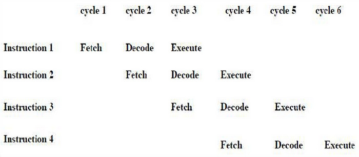
When using CISC, each steps might not take a consistent 1-cycle-per-step. For the POLY operation, the execute step alone might take 10 cycles for an x2 expression. In CISC, it’s hard to get your operations lining up nicely and therefore it’s tough to get good performance on complex instructions.
Pipelining, in short, is the concept of interleaving these instructions concurrently.
Why is a CPU architecture migration tough?
Apple and the AIM alliance hatched their scheme.
PowerPC, a modern Reduced Instruction Set Computer microprocessor architecture, was built to compete directly with the dominant Intel x86 architecture.
PowerPC promised better efficiency — that is, more CPU operations per watt of electricity — and since Apple controlled both software and hardware, they could optimise the Mac OS for this processor architecture.
Now they just had to migrate their ecosystem.
Assembly Language
Software written for one processor doesn’t necessarily run on another. Different families of processors naturally contain different instruction sets — that is, the list of assembly instructions that define each CPU operation.
Here’s a slice of Motorola 68k assembly code:
MOVE.L $1000, D0 ; Load longword from address $1000 into data register D0 MOVE.L $1004, D1 ; Load longword from address $1004 into data register D1 ADD.L D1, D0 ; Add the values in D0 and D1, result stored in D0 MOVE.L $1000, D0 ; Load longword from address $1000 into data register D1 NOT.L D1 ; Invert all bits in D1And now, here is what PowerPC assembly code looked like:
lwz r3, 0x1000 ; Load word from address 0x1000 into register r3 lwz r4, 0x1004 ; Load word from address 0x1004 into register r4 add r5, r3, r4 ; Add the values in r3 and r4, result stored in r5 lwz r3, 0x1000 ; Load word from address 0x1000 into register r3 not r4, r3 ; Invert all bits in r3 and store the result in r4Since the machine instructions themselves are different, all the existing software in Apple’s ecosystem would need to be re-compiled, and in some cases re-written (such as when writing compiler software, or when code makes assumptions about endian-ness), in order to work on PowerPC machines.
Apple needed a plan.
The PowerPC Transition
Apple developed two strategies to manage this transition:
A Emulator was developed where PowerPC could emulate the Motorola CPU. This translates instructions from one instruction set architecture to another in real-time.
This, unsurprisingly, incurs a huge performance cost. Fortunately, since the PowerPC CPUs were so powerful, emulation wasn’t usually a massive issue for consumers who were upgrading their hardware.
Another strategy which Apple employed was to use “fat binaries” for software during the transition period. This allowed software to contain code compiled for both 68k and PowerPC architectures. Therefore, engineers could ship a single app which worked on both Mac CPU platforms by containing two separate binaries.
In the era when 80MB was a decent hard drive, this was pretty annoying, so a cottage industry of binary stripping tools spawned so end-users only needed to save the one that worked on their device.
Overall, Apple’s migration was a success. Moving from 68k to PowerPC lent a massive performance boost. Emulation and fat binaries allowed the software ecosystem to transition without a major hitch.
Unfortunately, the Wintel alliance was barely touched. Their market dominance grew to unprecedented levels with the release of Pentium and Windows 95. Windows grew into the default computing platform, tragically transforming school ICT curriculums the world over into “how to use Microsoft Office”.
Now that they had a solid hardware platform, Apple’s antiquated System 7 Mac OS became the primary headwind. Internal projects to create a modern competitor to Windows had failed, which meant an acquisition was the only way out of a tailspin — simply buying a new OS.
This laid the groundwork for Apple’s purchase of NeXT and the return of Steve Jobs.
2006 — Intel x86
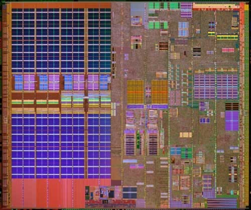
By the early 2000s, Apple had its mojo back.
Jobs is CEO. An era-defining software transition to Mac OS X had been a success. The iPod has turned a struggling computer company with single-digit market share into a consumer electronics powerhouse.
Desktops dominated the 80s, the 90s, and the turn of the millennium. But as Moore’s Law marches inexorably onwards, electronics are miniaturising and laptops are becoming big business.
When your hardware isn’t connected to mains electricity, battery becomes a bottleneck. With performance-per-watt the foremost concern, one thing became clear in the early 2000s: PowerPC architecture was failing to keep pace behind the Intel x86 behemoth.
Intel had simply been out-executing, out-manufacturing, and out-R&D-ing the competition. Their vast installed base of Windows hardware granted an unbeatable ecosystem of compatible software, and printed money to further invest in deepening the Intel processor technology moat.
The early-2000s PowerPC CPUs used far too much power and generated far too much heat to create the ultra-thin MacBook Air that Jobs was envisioning. With more than 50% of their revenues already drawn from laptop computers, the decision was clear: to compete, Apple had to switch to Intel.
WWDC 2005
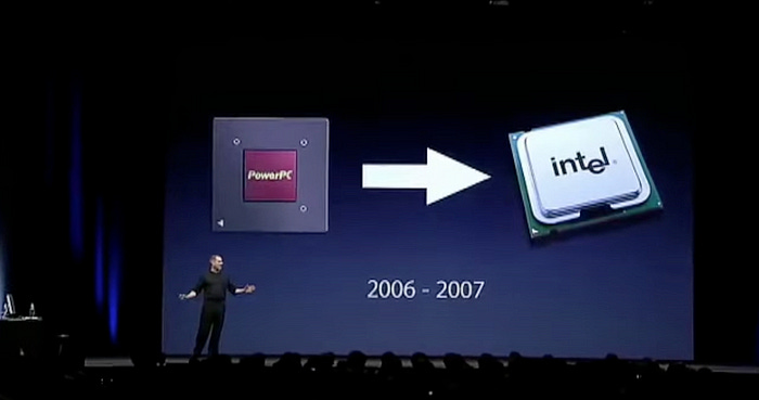
Jobs explained it best at Apple’s 2005 Worldwide Developer Conference:
“I stood up here two years ago in front of you and I promised you a 3 GHz Mac, and we haven’t been able to deliver that to you yet.
... As we look ahead we can of envision some amazing products we want to build for you and we don’t know how to build them with the future PowerPC roadmap.”
But my favourite part of the video?
“So get on Xcode 2.1 and get your copy today. There will be a copy for everybody at the registration desk immediately following this keynote.”
As someone who became a developer in the 2010s, picking up a CD at a conference for your latest Xcode update seems so quaint. I wonder if the 2005 Betas were as glitchy as we are used to today.
What really fascinates me, however, is this:
What made Intel x86 CPUs so much better?
Intel x86 processors are descended from a family of instruction set architectures pioneered in 1978 with the Intel 8086. Future processors, such as 1982's Intel 80186 or 2000’s Pentium 4, maintained backwards compatibility with this original instruction set. You’re reading that right: a program compiled on 8086 in the 70s would run fine in the 2000s without any modification.
But software ecosystem is just part of the story.
By 2006, high-end Intel x86 processors were projected to produce almost 5x the performance per watt compared to PowerPC, and nearly 1.5x the clock speed.
Intel was innovating on all aspects of their CPUs, such as:
- CPU Caches (L1, L2, and L3)
- Branch Prediction
- Superscalar Architecture
Let’s go over these in some detail, since they are really important concepts in modern CPU performance. No piece single-handedly made Intel’s x86 the winner — the interconnected nature of a CPU meant that optimisation across all these components (and more) kept x86 ahead of the pack.
CPU Caches
As previously explained, a CPU takes data from memory (RAM), places it in ultra-fast registers on the processor chip, and performs operations on that data. But at gigahertz clock speeds (1,000,000,000 operations per second), fetching instructions and data from RAM is far too slow.
Therefore, CPUs evolved on-chip caches to store middling amounts of data. These act as intermediary miniature blocks of RAM, stored physically closer to the chip itself, and allow for faster access to the necessary data.
These caches are themselves tiered:
- The L1 Cache is the smallest, fastest tier — directly integrated with the CPU core to store a small amount of data (a few kB) for rapid retrieval. Since these are integrated so close to the processor circuitry itself, there is an L1 Cache for each CPU core.
- The L2 Cache is the middle layer, balancing speed and capacity, usually integrated somewhere on the CPU chip itself (and like all middle siblings, usually left to the side). This cache could be partitioned for each CPU core, or shared between them all.
- The L3 Cache is the final buffer before the dreaded cache miss forces the CPU to search for data in RAM — a pyrrhic round-trip across the motherboard and back. This tier of storage is a shared memory pool of many megabytes between all CPU cores.
This diagram from Harvard’s CS course explains better than I ever could:
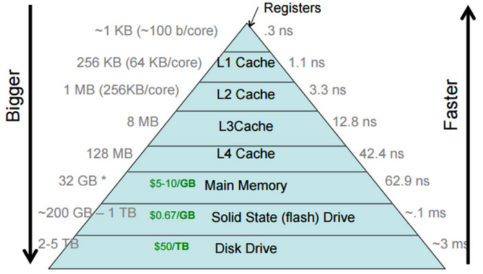
Whenever a CPU needs to fetch instructions or data that isn’t stored in the nearest cache, it’s known as a cache miss. It needs to fetch from the next tier of cache, or the next tier, or RAM, or disk! This can badly impact speed and efficiency.
As a macro-scale analogy, consider how slowly your app appears to load when your program has to look for data over the network, instead of from local storage. Round-trips on the nano-scale of a CPU can add up quickly.
By the mid-2000s, Intel’s x86 CPU caches dwarfed those on PowerPC, meaning lower latency and better performance. When supplemented with improved pre-fetching and predictive algorithms, expensive cache misses became less of a problem on x86.
These in turn improved performance-per-watt because when data is next to the processor, less electricity is physically being moved through the CPU’s circuitry to move bytes of memory around.
Branch Prediction
Branch Prediction sounds like arcane, occult magick when you first hear about it.
Branch instructions are the assembly code versions of conditional statements such as if/else — manifesting on the processor as jumps, calls, and returns. Clever CPUs use statistics to guess where the code is going, and try to keep the instruction pipeline filled for maximum utilisation.
The mechanism for this involves hardware algorithms built directly into the circuits of the CPU. A buffer called the Branch History Table caches recent branch outcomes. Patterns are analysed to draw predictions.
Advanced branch predictors apply the ultimate YOLO method: speculative execution, where instructions on the predicted branch are executed before the outcome is confirmed.
Intel’s silicon crystal balls helped the x86 processor go far faster than non-psychic CPUs.
Superscalar Architecture
Superscalar architecture is the ultimate in multitasking. Superscalar CPUs can simultaneously execute multiple instructions during a single clock cycle:
- In the fetch phase, the CPU collects multiple instructions from the operation pipeline.
- The decode phase utilises multiple decoder units to evaluate each instruction.
- These instructions may be dispatched to different execution units of the CPU.
This architecture works because operations such as arithmetic, moving memory between registers, and floating-point operations require different pieces of circuitry on the ALU. Therefore, if you’re clever, several instructions can be performed in parallel.
This is a tough process to get right. Bottlenecks can occur if multiple simultaneous operations need to use the same resource such as the same register or the same ALU adder circuit. Dependency issues can also lead to stalls, especially if an instruction is stuck waiting on the result of another longer-running operation.
Intel had the will and, more importantly, the R&D dollars, to get superscalar architecture working effectively on their CPU cores.
Further Intel Innovations
As well as caching, branch prediction, and superscalar architecture, Intel’s x86 chips further optimised many features of their CPUs:
- Advanced pipelining that split the fetch, decode, execute cycle into up to 21 stages that allowed for far more instructions to run per second at a given clock speed.
- Increased numbers of execution unitsin the ALUs to allow for easier parallelisation of operations from superscalar architecture.
- Hyper-threading which allowed a single CPU core to present to the OS as 2 logical cores, enabling one core to execute 2 threads simultaneously.
Apple’s Intel Migration Strategy
Apple again employed their time-honoured transition techniques for a smooth CPU architecture migration.
Apple introduced universal binaries built for both CPU architectures, which could be set up with a simple Xcode build configuration.
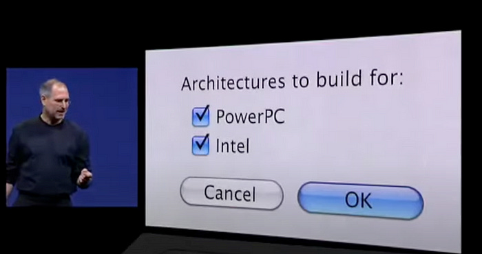
Apple also introduced Rosetta, a dynamic binary translator which Apple described as “the most amazing software you’ll never see”. It was embedded in Mac OS X Tiger, the first OS released on x86 Macs, and allowed PowerPC apps to run on x86 automagically.
Apple goes very far out of their way to explain that Rosetta is not an emulator — Rosetta dynamically translates code ‘on the fly’ as your program runs. In practice, what this meant was that PowerPC CPU instructions and OS system calls from the application binary were translated into equivalent x86 assembly and syscalls.
Apple under-promised with a years-long transition timeline and over-delivered way ahead of schedule, fulfilling Jobs’ dreams of tiny form factors and bringing Apple into the modern age.
2020—Apple Silicon
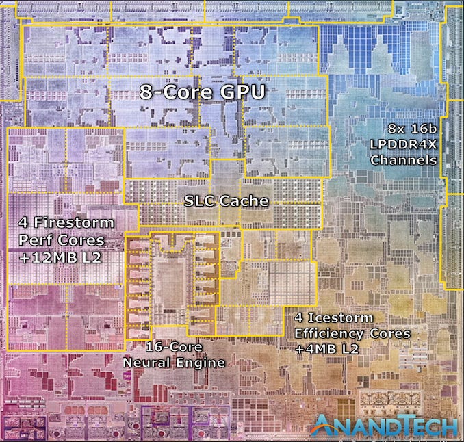
Anyone who’s read Walter Isaacson’s book on Jobs will know Apple’s ethos, and their ultimate competitive advantage: the tight integration of hardware and software to produce insanely great products.
Reliance on Intel for x86 CPUs meant a sometimes painful dependency on Intel’s supply constraints and release delays which sometimes impacted Apple’s roadmap.
For decades, the CPU had been the one that got away. From the off-the-shelf MOS 6502 microprocessor of the Apple I to the high-end Intel Xeon CPU of the 2019 Mac Pro, Apple never truly owned this part of the value chain.
But now, they could.
The O.G. 2G iPhone released in 2007 with an ARM CPU supplied by Samsung. At the turn of the decade, however, from the iPhone 4, Apple began to design its own chips, starting with the A4.
Apple iterated. And then continued to iterate.
2020.
The iPhone is the god of all cash cows.
Apple, now the most valuable publicly-traded company on the planet, is plowing $20,000,000,000 of cash flow into R&D like it’s nothing.
The seriously long-term
Wait a moment — before we get to the present day, we need to go back in history a bit. This might get bumpy.
In 2008, Apple purchased P.A. Semiconductor for $278m, a CPU design company known for high-end low-power processors. P.A.’s CPUs were originally based on IBM’s Power architecture — the very same instruction set used by the AIM alliance in the PowerPC Macs.
At the time, Android OS was entering the smartphone market. Owning its own chip designs would allow the iPhone to differentiate further from competitors in the newly crowded market. The acquisition also allowed Apple, famous for its obsessive degree of secrecy, to keep its best proprietary chip designs hush-hush in-house.
This acquisition was supplemented a decade later, in 2018, with a partial acqui-hire of Dialog, a European chip designer, for $300m.
Alright, can we talk about M1 now?
No. First, we must go back even further.
ARM’s RISC instruction set and chip designs are dominant today. ARM was in fact founded in 1990 as a joint venture between Apple and Acorn Computers. Legend has it — and by legend I mean this unsourced claim on Quora — that Steve Jobs convinced Acorn to abandon their hardware products and focus on low-power processor design.
I want to believe it, because it’s just perfectly emblematic of the long-term thinking that made Apple what it is today.
Anyway. You follow? Grand. Back to 2020.
The Dawn of Apple Silicon
Apple Engineers had been designing and iterating upon the ARM chips in the iPhone and iPad for years.
Due to the mobile form factor — it’s tough to fit cooling fans in your pocket — power consumption and heat efficiency are the big concerns. RISC architecture is the clear answer to this, supplanting the x86 giant in mobile use cases.
And by 2020, these ARM CPUs had been improving fast.
Way faster than Intel’s x86 chips.
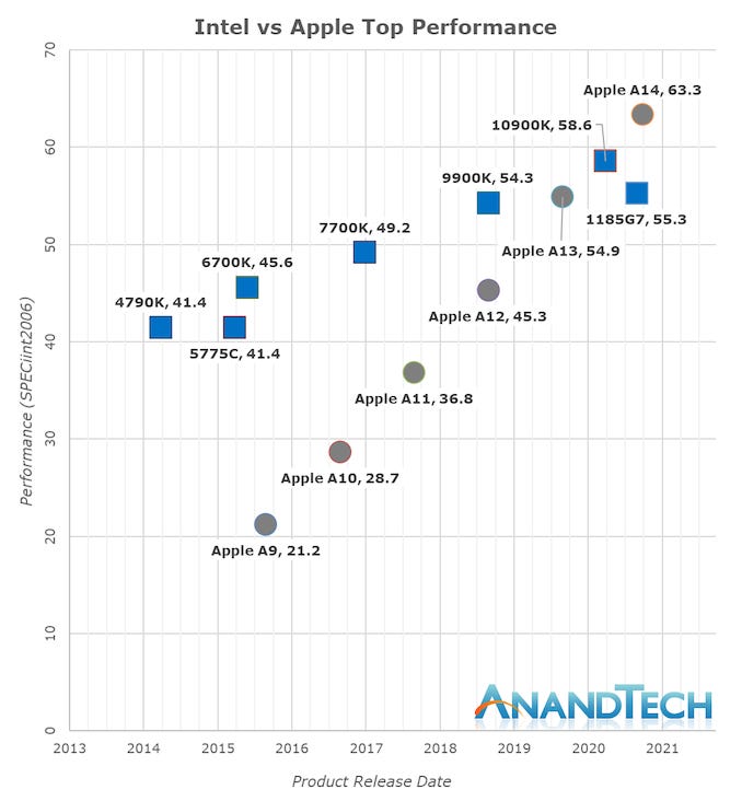
Apple’s custom ARM CPUs had improved to the point where there was no question about it—they was powerful enough to use in Apple laptops.
In 2020, Apple announced its third great Mac CPU architecture transition with the M1 — heralding the age of Apple Silicon.
What exactly is an M1?
The M1 was the first iteration of the “M family” of Apple Silicon chips, their custom hardware for Mac laptops and desktops. It has siblings such as the M1 Pro, the M1 Max, and the M1 Ultra. Today, you can even buy M2 chips in the latest hardware (but I’m holding out for M3 before I start petitioning my CTO).
The M1 is a system-on-a-chip (SoC). This is an approach to building hardware that differs from standard desktop PCs. Instead of mounting interchangeable components on a motherboard (such as CPU, storage, RAM, graphics card), SoCs integrate everything into a single component, which is why the approach lent itself naturally to space-constrained mobile devices.
Upgrading to an M1 MacBook for the first time is like magic. A real game-changer. Everything is lightning-fast, the cooling fan never seems to switch on, and the battery lasts all day on a single charge.
How is the M1 so powerful, when using so little power?
The M1’s Secret Sauce
As mentioned in the Intel section, the interconnected nature of a CPU usually makes it tough to evaluate outperformance between chip architectures.
Intel’s primary performance driver has been to shrink transistors and fit more, faster, CPU cores onto the chip. More, faster, CPU cores leads naturally to higher performance.
But in the case of the M1, there is a completely different approach which leads to its outperformance: Specialisation.
Heterogeneous Computing
The M1 chips apply a heterogeneous computing strategy. This means specialised components for specific workloads. PC gamers are already familiar with this. For decades, Nvidia has been selling graphics cards — GPUs — to handle the specialised parallel workloads you encounter with videogame rendering engines.
Apple takes this approach to the next level with a radical shift in the direction of heterogeneous workloads. The components of the M1 SoC are specialised for many computing tasks:
- Image processing circuitry
- Mathematical signal processors
- AI-accelerating neural engines
- Dedicated video encoder and decoders
- A secure enclave for encrypted storage
- 8 GPU cores with 128 parallel execution units
- 4 high-performance Firestorm CPU cores
- 4 efficient, low-energy Icestorm CPU cores
This approach to utilising twin sets of CPUs was coined by ARM as big.LITTLE architecture, which optimises power consumption for those general CPU workloads not dispatched to specialist components.
The Firestorm CPUs relentlessly execute time-sensitive workloads requested by the user; while the Icestorm CPUs handle background workloads more slowly while consuming 90% less power.
As well as the core heterogeneous architecture of the Apple Silicon SoC, there are some further supplementary reasons for the astonishing M1 performance:
- Unified Memory Architecture
- Out-of-order Execution
- Physics: The Ultimate Constraint
Unified Memory Architecture
The M1 chips have a unified memory architecture shared between GPU and CPUs. This is a masterstroke for performance. When sending data to an external GPU for processing, a CPU usually needs to copy data into the memory owned by the GPU, before it could be picked up for processing.
This is the problem Metal was introduced to solve — intermediary translation of a graphics driver utilises the CPU, which introduces a serious performance bottleneck when you really want graphics instructions to go to the GPU.
Interested? Read more in my previous entry in this series, Through the Ages: Apple Animation APIs.
Why don’t all processors have integrated graphics?
In order to get this right, Apple had to solve two major problems that arise when integrating CPU and GPU onto a SoC:
- CPUs and GPUs like their data formatted differently. CPUs love to nibble small bytes little and often, GPUs like to guzzle massive blobs of data, infrequently, for massively parallel processing.
- GPUs make heat. A lot of heat. This is why graphics cards have integrated cooling fans for that “jumbo jet” aesthetic.
Apple’s approach allocates the same blocks of memory — both RAM and L3 cache — shared between both processors, in a format that can supply big chunks that the GPU likes at the high throughput that the CPU requires. Their ARM chips are low-energy enough to integrate on the same die without melting a hole through your lap(top).
Out-of-order Execution
While the heterogeneous architecture allows specialised workloads to go to the best tool for the job, the Firestorm CPU cores themselves are extremely powerful for general workloads.
We previously discussed superscalar architecture that enabled CPU cores to simultaneously fetch, decode, and dispatch multiple instructions at once. The M1 chips, by virtue of their RISC architecture, allow Apple to take this to the next level with out-of-order execution.
ARM RISC instructions are all 4 bytes long (32 bits), while x86 CISC instructions vary from 1–15 bytes. This means ARM chips can easily split up a continuous stream of instruction bytes straight to decoders without any analysis overhead.
The basic M1 chip has an insane 8 decoders, which the Firestorm CPU cores fill simultaneously each clock cycle. These instructions are dispatched in parallel to its various specialised pieces of circuitry.
Apple Silicon analyses a dependency graph between hundreds of instructions at once, so it knows what can be dispatched now and what needs to wait on results. Pair this with its advanced branch prediction, and the M1 CPU is essentially burning Atium.
Physics: The Ultimate Constraint
There is one final reason this SoC is so fast and so power-efficient. It’s the same concept we looked at when learning about CPU caches.
Simply put, everything on the M1 chip is physically so close together. Even with electrical signals moving literally at lightning speed, operations are simply faster when there is less distance to travel.
At GHz clock speeds, those nanoseconds add up.
Ultra high-performance
For the M1 Ultra chips, designed to give the maximum output, Apple took a more blunt instrument out of its tool-belt. Instead of an extreme ultraviolet lithography machine, Tim Cook took out a sledgehammer.
The M1 Ultra chip is simply two M1 Max chips stuck together.
It’s perhaps a little more subtle than that — the bridging structure enables a pretty inter-chip throughput of 2.5TB/s, which allows the components to behave exactly as if they’re the same chip.
Apple’s Final Transition?
Apple continued to apply its battle-tested approach for the transition from Intel x86 to Apple Silicon.
Developers can build universal apps which contain both Intel and Apple Silicon binaries. Additionally, Rosetta has been upgraded to Rosetta II to invisibly interpret Intel instructions into ARM on-the-fly.
Grandiose as always, Apple claims that some Intel apps and games will perform better on ARM using Rosetta II than they did on their original.
The Death of Intel?
It was a painful blow to Intel for one of their biggest customers to break off their longstanding partnership. Intel is somewhat in denial of reality and is pretty sure they can catch up by investing further in their own.
Between Apple Silicon and the dominance of Nvidia for AI use cases, one thing is clear: Intel has been too complacent for too long.
“Success breeds complacency, complacency breeds failure, only the paranoid survive”
Andy Grove, Intel Co-Founder
Conclusion
Originally, this was meant to be a brief history of Apple’s famous CPU architecture migrations, however as usual my curiosity kind of got away from me. I was frustrated with the surface-level depth of most of my information sources.
- I had to know why the Macintosh team picked Motorola 68k over the available options.
- I had to know what made a migration to a new CPU architecture like PowerPC so difficult.
- I had to know what actually caused Intel’s x86 architecture to be so far ahead of its competition.
- I had to know how on Earth the M1 chips were so damn efficient.
I reckon I did a pretty good job.
I hope you learned a little, and most importantly, had some fun on the way.
Have you used any of these architectures before? Perhaps you’ve written assembly for them, used the CPU as a component in a custom build PC, or perhaps even just been amazed at your new M1 Mac? Share your story in the comments!
If you liked this piece, check out my other entry in my Through The Ages series: Through the Ages: Apple Animation APIs.